

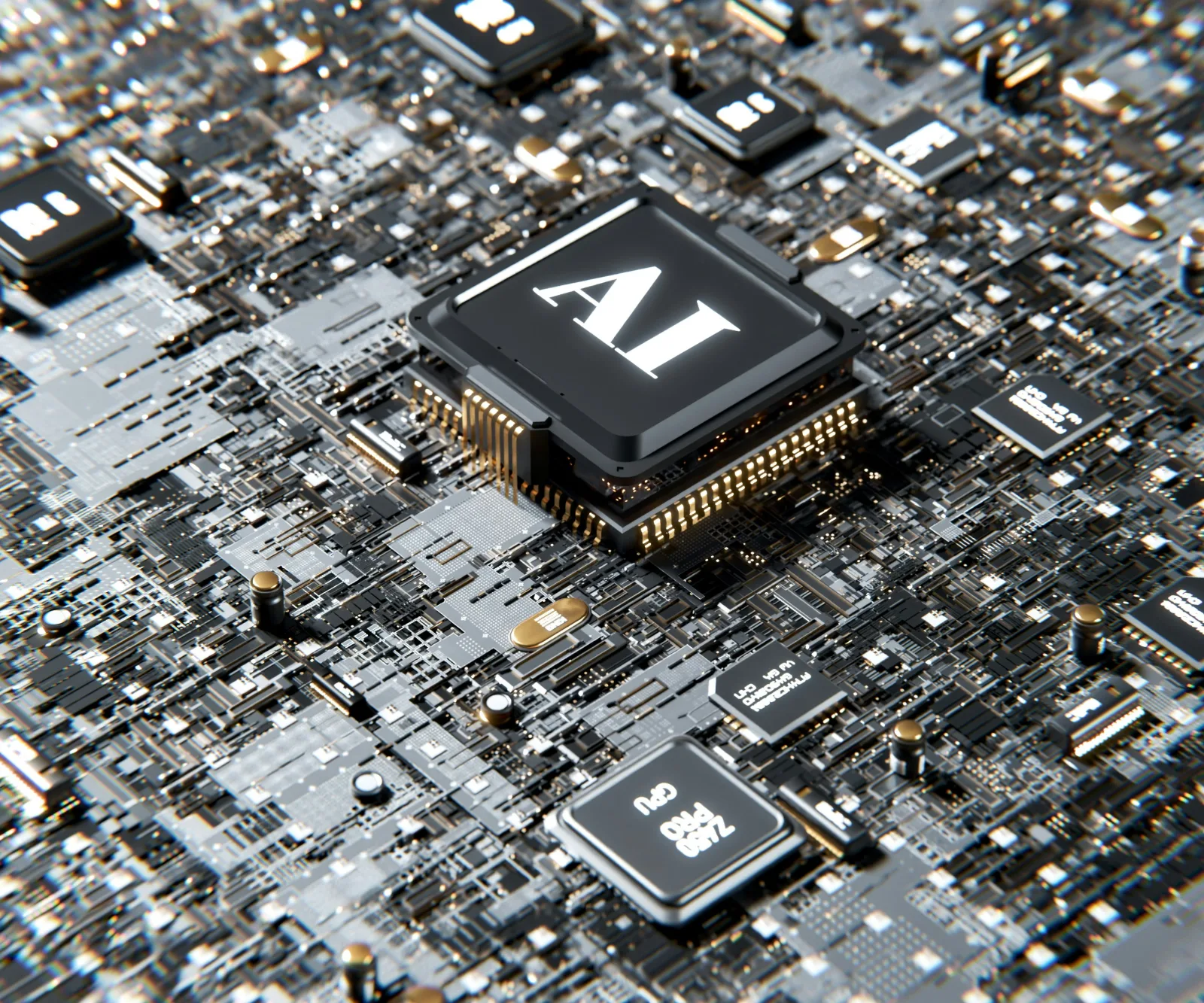
The trajectory of mobile system-on-chip (SoC) design has fundamentally shifted from raw clock speed increases toward specialized, power-efficient heterogeneous computing. As mobile operating systems rely more heavily on real-time generative models, multimodal processing, and contextual awareness, the silicon powering these workloads must evolve rapidly. Examining the transition from the A19 architecture to the next-generation A20 chip highlights how semiconductor foundries and chip designers are optimizing hardware specifically for complex artificial intelligence integration.
Lithography Advances and Architectural Efficiency
The foundation of every generational leap in mobile silicon is the underlying fabrication process node. While the A19 chip leveraged an advanced 3-nanometer class node (N3P) to achieve strong energy efficiency and sustained clock stability, the A20 platform shifts toward next-generation lithography refinements, incorporating TSMC’s 2-nanometer (N2) process technology alongside advanced backside power delivery networks (BSPDN).
This transition allows transistor density to scale higher without increasing physical die size or thermal footprint. By decoupling power distribution lines from signal interconnects on the front of the wafer, the A20 reduces internal resistance, allowing CPU and GPU cores to maintain peak performance states longer before hitting thermal throttling limits.
Read Also: Design and Display Refinements: What Changes Between Generations?
CPU and GPU Architecture: Balancing Compute and Graphics
To handle complex computational demands, both the A19 and A20 feature high-performance and high-efficiency CPU core arrangements, paired with custom GPU clusters. However, their internal execution pipelines differ significantly:
- A19 Architecture: Optimized for wide execution width, high IPC (instructions per cycle) efficiency, and hardware-accelerated ray tracing for graphical fidelity.
- A20 Architecture: Features redesigned execution units, expanded L2/L3 cache allocations, and specialized matrix math acceleration within both the CPU microarchitecture and GPU compute units.
+-----------------------------------------------------------------------+
| A19 Architecture: Standard Compute + Neural Engine Interconnect       |
+-----------------------------------------------------------------------+
                                   │
                                   ▼ (Hardware Matrix Acceleration)
+-----------------------------------------------------------------------+
| A20 Architecture: Unified Memory Architecture + On-Die Matrix Accelerators |
+-----------------------------------------------------------------------+
This structural shift in the A20 enables faster floating-point operations ($FP16$ and $INT8$), which directly benefits both heavy mobile gaming workloads and localized machine learning inference.
Neural Engine Throughput and On-Device AI Acceleration
The most critical distinction between the two chip generations lies in their dedicated Neural Engine capabilities. While the A19’s 16-core Neural Engine provided robust performance for localized natural language processing and computer vision tasks, the A20 introduces a redesigned Neural Processing Unit (NPU) architecture tailored specifically for Large Language Models (LLMs) and diffusion models running natively on-device.
By increasing operational FLOPS (floating-point operations per second) and increasing memory bandwidth, the A20 allows on-device AI assistants and generative features to process multi-turn queries with significantly lower latency. This hardware acceleration reduces reliance on cloud servers, improving response times, battery endurance, and user data privacy.
Memory Bandwidth and Unified Memory Integration
A common bottleneck in mobile AI execution is memory bandwidth. Running multi-billion parameter models requires rapid data retrieval from system RAM to the NPU and GPU without causing memory bus congestion.
The A19 platform addressed this with high-bandwidth LPDDR5X memory support. The A20 builds upon this architecture by increasing memory interface speeds and integrating dynamic memory compression algorithms directly into the unified memory controller. This ensures that background AI operations do not starve graphical rendering or system-level multitasking of essential memory throughput.
Conclusion
The evolution from Apple’s A19 to the A20 silicon reflects a broader industry transition toward AI-centric semiconductor design. Through process node refinements, increased unified memory bandwidth, and a re-engineered Neural Engine, the A20 delivers substantial upgrades in on-device AI capabilities and power efficiency. For power users and tech enthusiasts, these architectural advances translate into faster local machine learning processing, improved battery longevity, and superior sustained system performance.
Sources / References:
- Semiconductor foundry fabrication roadmaps and technical whitepapers on advanced node processes.
- System-on-Chip (SoC) microarchitecture breakdowns and hardware benchmarking analyses.




Komentar 0
Belum ada komentar. Jadilah yang pertama berkomentar!